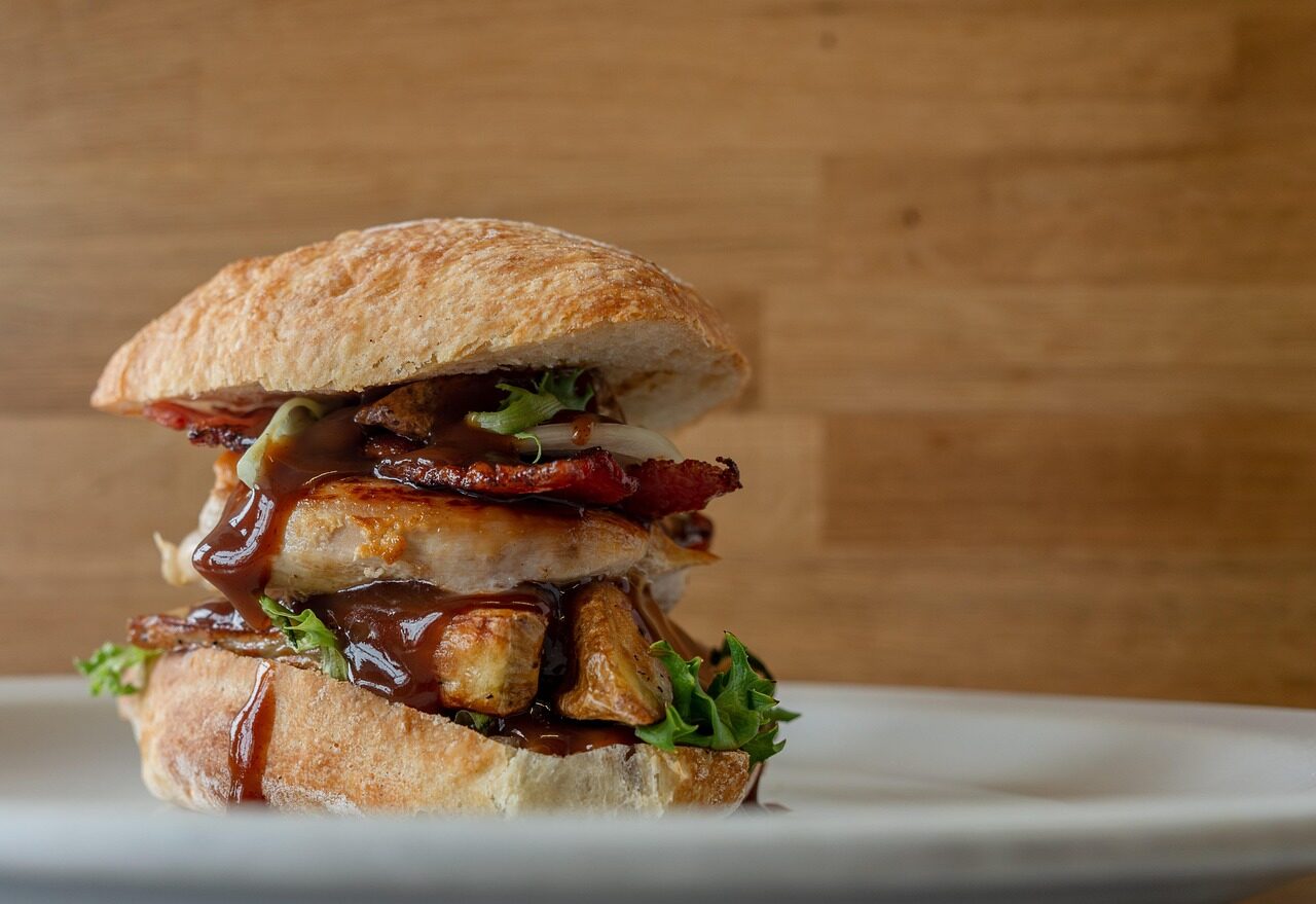
In der Gastronomie wird der Burger oft als „einfaches Gericht“ unterschätzt. Auf den ersten Blick scheint es nur um Fleisch, Sauce und ein paar Toppings zu gehen. In der Realität entscheidet jedoch ein oft unterschätzter Faktor über Erfolg oder Misserfolg des gesamten Produkts – das Burgerbrötchen.
Gerade im täglichen Betrieb zeigt sich, dass selbst kleine Fehler bei der Auswahl große Auswirkungen haben können: instabile Burger, unzufriedene Gäste, unnötiger Food Waste und im schlimmsten Fall ein beschädigter Markenauftritt.
Warum die Wahl der Burgerbrötchen oft unterschätzt wird
Viele Gastronomiebetriebe investieren viel Zeit in die Entwicklung von Rezepturen, Saucen und Fleischqualität. Das Brötchen wird dabei häufig eher als „Träger“ betrachtet, der einfach funktionieren soll.
Doch genau hier entsteht das Problem. Das Brötchen ist nicht nur Verpackung, sondern ein aktiver Bestandteil des Geschmackserlebnisses. Es muss gleichzeitig weich und stabil sein, Feuchtigkeit halten, ohne durchzuweichen, und optisch ansprechend bleiben – vom Pass bis zum Gasttisch.
In der Praxis zeigt sich schnell: Wenn das Brötchen nicht passt, verliert selbst der beste Burger an Qualität.
Fokus nur auf Preis statt auf Qualität
Einer der häufigsten Fehler in der Gastronomie ist die rein preisgetriebene Auswahl von Produkten. Gerade bei hohem Verbrauch wirken kleine Preisunterschiede pro Stück zunächst entscheidend für die Kalkulation.
In der Realität führt dieser Ansatz jedoch oft zu Problemen im täglichen Betrieb. Günstigere Brötchen sind häufig weniger stabil, verlieren schneller ihre Struktur oder reagieren empfindlich auf Saucen und Hitze. Der Burger beginnt bereits nach wenigen Minuten auseinanderzufallen oder wirkt optisch unattraktiv.
Das führt nicht nur zu Reklamationen, sondern auch zu einem indirekten Kostenanstieg: mehr Remakes in der Küche, höhere Lebensmittelverschwendung und geringere Kundenzufriedenheit. Viele Restaurants stellen erst nach einiger Zeit fest, dass der scheinbar günstigere Einkauf am Ende teurer wird als ein hochwertiges Produkt.
Keine Berücksichtigung der realen Küchenbedingungen
Ein weiterer typischer Fehler entsteht bereits in der Auswahlphase: Produkte werden getestet unter idealen Bedingungen, nicht unter realen Belastungen des Gastronomiealltags.
Im Alltag sieht die Situation jedoch ganz anders aus. In Stoßzeiten müssen Burger in hoher Geschwindigkeit produziert werden. Gleichzeitig werden sie oft verpackt, transportiert oder geliefert. Temperatur, Feuchtigkeit und Zeit spielen dabei eine entscheidende Rolle.
Ein gutes Burgerbrötchen muss genau für diese Bedingungen entwickelt sein. Es darf nicht nur im perfekten Setup funktionieren, sondern auch nach zehn Minuten im Takeaway, unter Hitze im Pass oder bei hoher Produktionslast stabil bleiben.
Wenn diese Faktoren nicht berücksichtigt werden, entstehen genau die Probleme, die viele Küchen täglich erleben: instabile Produkte, ungleichmäßige Qualität und unnötiger Stress im Service.
Instabile Lieferqualität und fehlende Konstanz
Einer der kritischsten Punkte in der professionellen Gastronomie ist die Konstanz. Selbst ein sehr gutes Produkt verliert seinen Wert, wenn es nicht zuverlässig gleich bleibt.
Viele Betriebe arbeiten mit mehreren Lieferanten oder wechseln regelmäßig, um Preise zu optimieren. Dadurch entstehen jedoch Schwankungen in Größe, Struktur oder Frische der Brötchen. Für die Küche bedeutet das: Jeder Burger verhält sich anders.
Diese fehlende Standardisierung erschwert nicht nur die Produktion, sondern auch die Qualitätssicherung. Gäste erwarten jedoch genau das Gegenteil – einen Burger, der immer gleich gut schmeckt und aussieht, unabhängig vom Tag oder Standort.
Falsche Auswahl des Brötchen-Typs für das Konzept
Nicht jedes Brötchen passt zu jedem Burger. Dieser Fehler entsteht besonders häufig bei der Entwicklung neuer Menüs oder bei der Expansion von Restaurants.
Ein zu weiches Brötchen kann bei saftigen Burgern schnell seine Stabilität verlieren, während ein zu trockenes Brötchen das gesamte Geschmackserlebnis negativ beeinflusst. Auch Größe und Verhältnis zum Patty spielen eine entscheidende Rolle, werden aber oft unterschätzt.
Das Ergebnis ist ein unausgewogenes Produkt, bei dem selbst hochwertige Zutaten nicht zur Geltung kommen. Gäste nehmen dies oft unbewusst wahr, was sich direkt auf Wiederbestellungen und Bewertungen auswirkt.
Keine ausreichenden Tests im realen Betrieb
Viele Entscheidungen werden auf Basis von Verkostungen getroffen, ohne das Produkt im echten Küchenalltag zu testen. Dabei unterscheiden sich Labor- oder Musterbedingungen stark vom späteren Einsatz.
Erst im Betrieb zeigt sich, wie sich ein Brötchen bei hoher Auslastung verhält: ob es stabil bleibt, wie es auf Saucen reagiert oder wie es sich bei Lieferung entwickelt.
Fehlende Tests führen oft dazu, dass Probleme erst auftreten, wenn das Produkt bereits eingeführt ist – ein Risiko, das im laufenden Geschäft schwer zu korrigieren ist.
Wie professionelle Gastronomie es richtig macht
Erfolgreiche Gastronomiebetriebe verfolgen einen klaren Ansatz: Sie betrachten das Brötchen nicht als Nebenprodukt, sondern als strategischen Bestandteil ihres Angebots.
Dabei stehen nicht kurzfristige Einsparungen im Vordergrund, sondern Stabilität, Wiederholbarkeit und Zuverlässigkeit. Produkte werden getestet, Lieferketten geprüft und langfristige Partnerschaften aufgebaut.
Viele Betriebe setzen bewusst auf spezialisierte Lösungen im BereichBrötchen für Burger, die genau für diese Anforderungen entwickelt wurden und auch unter hoher Belastung konstant funktionieren.
Das Burgerbrötchen als unterschätzter Erfolgsfaktor
Die häufigsten Fehler bei der Auswahl von Burgerbrötchen entstehen nicht aus mangelndem Interesse, sondern aus fehlender Priorisierung im täglichen Geschäft.
Wer jedoch versteht, dass das Brötchen ein zentraler Bestandteil des Produkts ist, kann Qualität, Effizienz und Kundenzufriedenheit deutlich steigern.
In der modernen Gastronomie entscheidet nicht nur das Rezept über den Erfolg eines Burgers – sondern die Stabilität jedes einzelnen Bestandteils.